HMI E.N.D. – Electronic Products Series
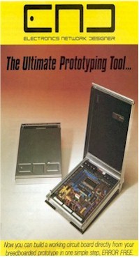
The HMI Hoyme END – Electronics Network Designer
The Patented Electronic Network Designer is a tool for the rapid prototyping of electronic circuits. It is comprised of a base matrix of high quality nickel silver Connector Clips in arrays of six, over which a printed Circuit Board is aligned. The designer prototypes the circuit through the board, using the clips to make the connections until the circuit is tested and ready for soldering. The circuit is soldered before being removed from the unit, and the painstaking process of transporting to a hard wired system is eliminated.
Operations Manual END-ED22-NDC – (pdf) – Small Size Designer – PDF(opens in New Window)
Operations Manual END-ED01-NAA – (pdf) – Full Size Designer – PDF(opens in New Window)
Circuit Board Schematic Worksheet-Full Size-END-CB-01AYF – (pdf) – PDF(opens in New Window)
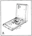
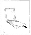 | The Circuit Board is inserted and held in place. |
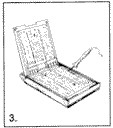
 | Components are inserted into the matrix to create the circuit. |
 | When completed, the product is turned over and all connections are soldered and trimmed. |
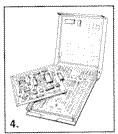 | The completed circuit board can then be removed from the product. |
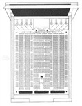 | Product Features: Compact Functional design Unit can be closed (with circuit board in process) for storage or transport Fits in Briefcase Conductive foam inside cover for safe storage of components All-metal Chassis construction for durability Improved Layout of Working Area Three separate working areas, two vertical, one horizontal Connection strips in rows of six (conventionally five) Over 3,400 Connection points 14 vertical buses 8 binding posts for inputs, accepts banana plug connectors Time Saving The E.N.D. patented system can save hours in the production of prototypes and short run or custom circuits Dimensions Circuit board – 6.875″ x 8.00″ x 0.031″ Electronics Network Designer – 7.75″ x 11.00″ x 1.25″ |
